

Click here for telephone inquiries.
TEL : 03-3969-3731
PRODUCTS
We are available up from prototype to mass production of the following
custom-made products that are based on customer’s demand.
Product information
Various optical lens
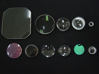
Processing the various types of lens utilizing the processing technology of industry-leading level corresponding to the high demands around the world.
we do coating and cementing, painting and semi-assemble, on request.
| Processing dimensions (outer diameter) | φ5mm~φ250mm |
|---|---|
| Outer diameter tolerance | 0/-0.015~ |
| Center thickness tolerances | ±0.015~ |
| Surface form | 1fr IRR 0.2 RSI 0.2~ |
| Centering error | 0.5‘~ |
| Surface imperfection | Scratch 1μm~ (Microscopy) |
Prism various
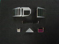
Industry is a top-level prism due to processing technology. From micro-prism to large planar substrate It offers services in accordance with the request of a wide variety of customers.
Fabricating materials
Optical glass, quartz, silicon, SUS, YAG, tungsten, fluorite, sapphire, titanium oxide, zirconia, alumina, germanium, etc.
| Processing dimension | 0.2mm ~ 200mm (Angle testplates is 30mm ~ 100mm) |
|---|---|
| Dimensional tolerance | ± 0.01mm ~ |
| Angular tolerance | ± 1 second to (1 minute Normal) |
| Surface accuracy: reflected wavefront | ~ λ / 50 (measurement wavelength 632.8nm) |
| Surface roughness | 2Å |
| Surface imperfection | Scratch 1μm ~ (microscopy) |
| Piramidaru | 5 seconds ~ |
Planar substrate
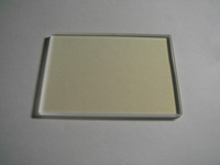
Polishing workable glass type
optical glass, ceramics, YAG, synthetic quartz, polycarbonate, silicon, SUS (metal), MgF2, sapphire, and other
Ultra-thin parallel planar substrate and ultra-precision cutting
Very product of atypical processed products and ultra-precision cutting of thin parallel plane substrate having a thickness of 0.08mm has been used in semiconductors, medical equipment and micromachine laser board.
| Processing thickness | 0.08mm ± 0.005mm ~ |
|---|---|
| Outer diameter tolerance | ± 0.01mm ~ |
| Parallelism | 0.5 seconds to |
| Surface form | Transmitted wavefront ~ λ / 10 (measurement wavelength 632.8nm) |
| Surface roughness | 2Å ~ 5Å |
| Surface imperfection | Scratch 1μm ~ (Microscopy) Dig 10μm ~ |
- Primary use
Medical equipment and optical communication equipment, optical switch micromachine
Large planar substrate
Large flat board has been used in laser relationship.
1 sided abrasive article surface accuracy ~ λ / 20 or less include (6 inches reference thickness instrument λ / 40) products that lighter up to 45% in the ribbed processed goods for the purpose of weight lighter.
| Outer diameter tolerance | ± 0.01mm ~ |
|---|---|
| Parallelism | 0.5 seconds to |
| Surface accuracy | Reflected wavefront ~λ / 40 (φ150) |
| Surface roughness | ~ λ / 10 (measurement wavelength 632.8nm) Surface roughness 2Å ~ 5Å |
| Appearance standard | Scratch 1μm ~ (Microscopy) Dig 10μm ~ |
Coating
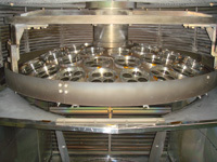
For Prism small prism angle prototype lens, you subjected to various coating processing.
- antireflection film (AR coat)
- reflective film
- polarizing film
- various filters
- transparent conductive film (ITO film)
- patterning
- water-repellent film
- hydrophilic film
Plastic packaging case
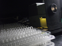
Mainly use for the storage and transport packaging container of optical lens, prism, wafer, electronic components and any parts.
Coating tool
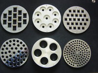
Tooling plate for coating.